Feature Analysis
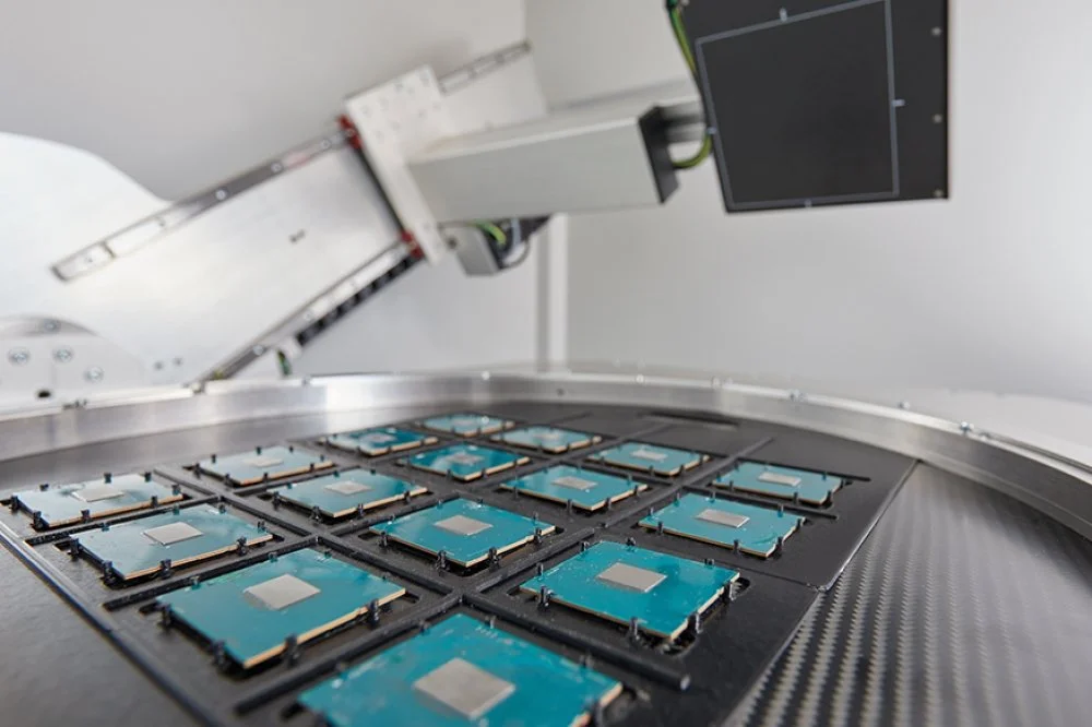
Level 1: External visual inspection
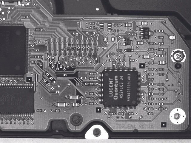
PCB and external component inspection
We detect burn marks, fractures, discoloration, and any signs of overheating or localized electrical failure.
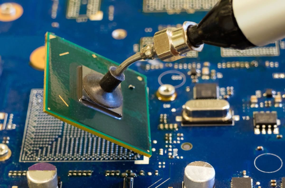
Solder joint stress testing
We evaluate solder thickening or cracking caused by mechanical stress that could compromise reliability.

Delamination detection
Through optical and acoustic inspection, we locate internal separations between the molding compound and the substrate.
Level 2: Non-Destructive Analysis
X-ray inspection
We check internal connections, solder joints, and possible shorts or discontinuities.

Optical and digital microscopy
We analyze surfaces at high magnification to reveal microdefects invisible to the naked eye.

Infrared thermography
We detect hot spots that indicate electrical leakage or overloading.
Level 3: Destructive and Laboratory Analysis
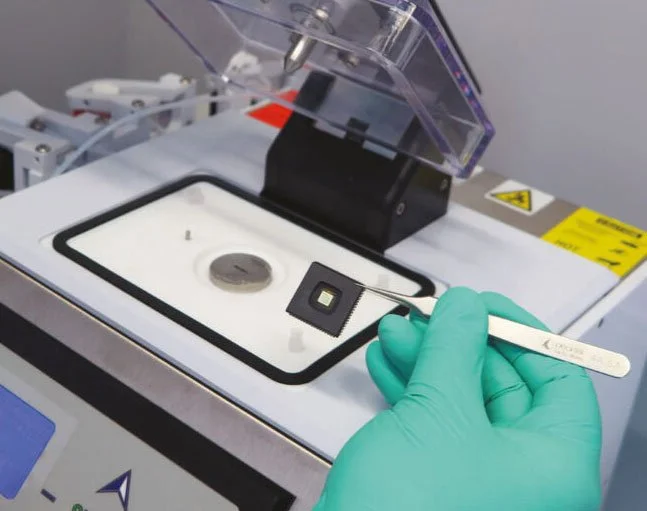
Chemical or mechanical decapsulation
We remove the package to expose the silicon die.

Scanning Electron Microscopy (SEM)
We study microscopic details such as fractures in tracks, metal migration, or contamination.
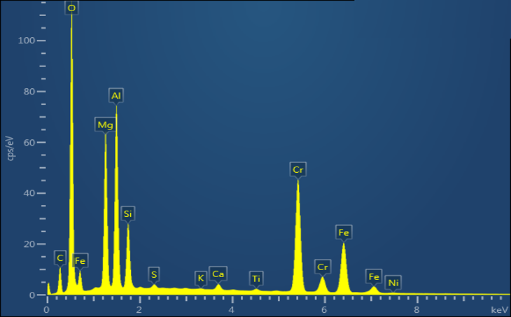
Energy Dispersive X-ray Spectroscopy (EDS/EDX)
We determine the chemical composition of residues or contaminants that caused the failure.

Request Your Quote Today
Ensure the reliability and performance of your electronic components with our professional Semiconductor services.
We provide the insights you need to make informed decisions and prevent costly failures.
Fast Response – Get your evaluation started within 24 hours.
Accurate Results – Backed by state-of-the-art equipment and certified experts.
Custom Solutions – Tailored to your industry and product requirements.

